Ever wanted to add a lot a flash memory to a small microcontroller? NOR flash or EEPROM are ok, but only for small size. For Gbit range, you need NAND, and with NAND comes CCR, LUT, wearleveling, etc… Furthermore, they are darn expensive in small volume.
SD and microSD card are very interesting: they cost nothing, and you just need a SPI interface as the controller is included.
Last night, I thought: “why not reflow a complete microSD card”, and save the cost of the socket, and PCB footprint size. As the card is composed of the same resin as chip casing and pins are flat bellow the microSD card and even gold plated, fore sure it should not be a problem to bring this to 270°C for 2-3 min….
Let’s try!
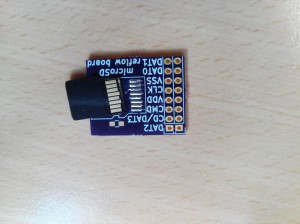
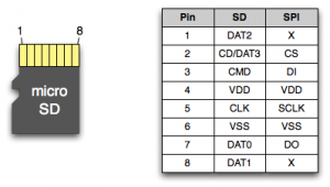 Then let’s create a small board, to try the reflow of a micro SD card and give access with some 2.54mm header.
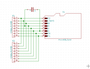
Lets open Kicad and start with the schematic with Eeschema:
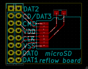
Then PCB new for the board layout:
MicroSD footprint and module for Kicad: microSD_Card
Let’s submit the gerber files to, you can order the board here (shared project): OSH Park
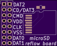 Total including USPS post mail: 4.10€
That was my fastest board made ever, 1h30 from searching the pinout to the confirmation email!
See you back in few week for the oven reflow test!
Update: the board and the reflow!
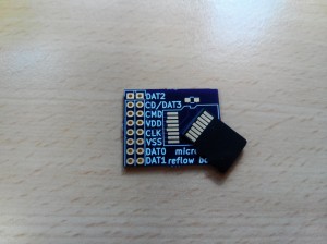 First, let’s clean it and apply some flux:
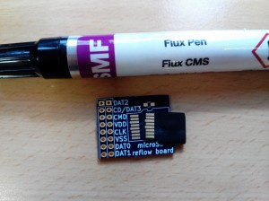 Then some solder on the pads, and flux again:
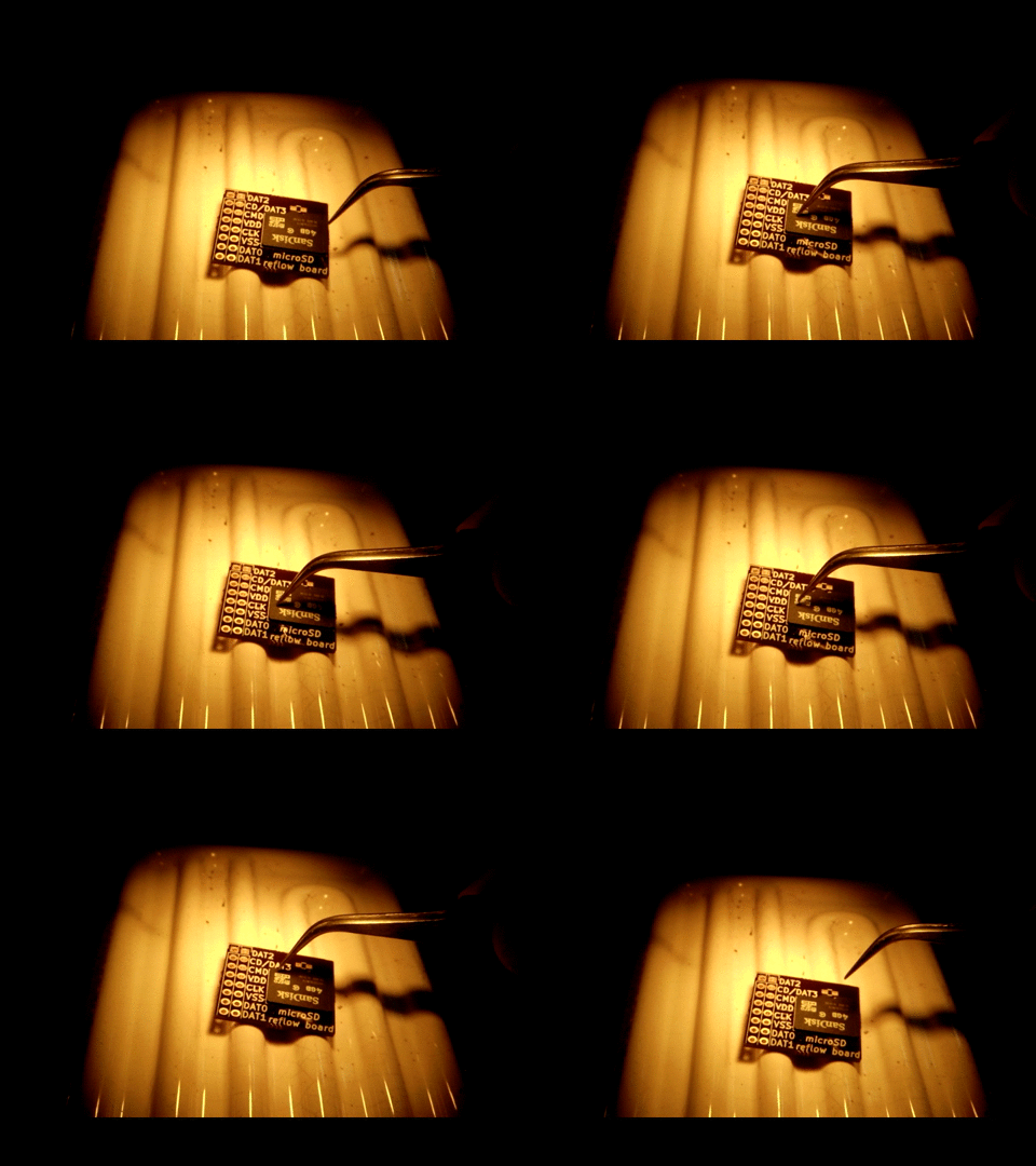
 Time to turn the heating plate and IR reflow on:
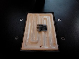 Just stir it a bit while it’s hot:
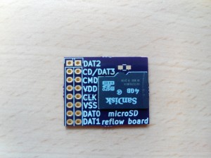
Houston, we have a reflow!
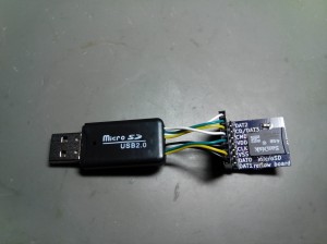
Then time to test: lets scavenge a super cheap reader microSD card reader:
And plug it: IT WORKS! After 3 min under the IR station, it does work.
I think I’ve to increase the pad size, in order to maximize the solder paste.
Now I’m confident sending to production, as I’ve quite a lot of theses cards in trays, ready for pick and place: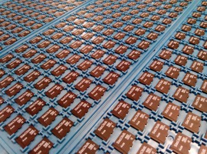

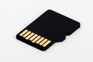
Did it work?
Hum, boards received but still have to find the time to try it!
Reflown and tested: it works!
Pingback: Reflow Solder Your Micro SD to Ensure it Doesnt Go Anywhere | Hackaday
Pingback: Reflow Solder Your Micro SD to Ensure it Doesnt Go Anywhere - Arduino collector blog
Pingback: Reflow Solder Your Micro SD to Ensure it Doesnt Go Anywhere | Ad Pub
Pingback: Reflow Solder Your Micro SD to Ensure it Doesnt Go Anywhere | Hack The Planet
Awesome! You could make the traces a little bigger from the pads as well just in case for better signal flow to the pads to the pins
Very cool idea and will be much more difficult for people to swipe those micro SD cards!
Hi,
Very good idea, really.
A note, you have the pins footprint flipped in the board
Pingback: Field Report: 2015-08-06 Retrieve Sensors from RioSecreto | Arduino based underwater sensors
Very interesting, I am working on similar design and worked out ok for the prototype. Did you do a production run reflow soldering the microsds? How did it go? Thanks!
So the plastics case is fine for reflow? Was there any sign of deformation?
Yes, no mark, and works fine, like any SMD component.
I didnt got to production with this, as it’s quite risky, and takes a lot of space.

At the end, I used the molex version where you can stuff component bellow the card:
Tweepy, why did you say everything was fine, and then suddenly say you didn’t use direct reflow in production because it was “risky?” What risk? We could really use your advice because we’re considering using the direct reflow technique in our product.
Everything was fine FOR ONE UNIT, but since it’s not even mentioned in the card’s DS, I cannot take the risk (30K€ BOM) with a 1k production.
Furthermore, as I said, my board was lacking space, with the molex connector, I was able to fit the MCU bellow the card.
But you can try it on a small batch (100 units), and come back with your results, I would definitely appreciate.
hey there
not sure if you can help me, but i’m trying to locate information (preferably as a file i can edit but i will settle for a drawing) to enable me to layout a pcb in the precise shape as a micro sd card (for a breakout board to slide into a microsd reader, which has a micro on it – for a mockup – not actual micro, just a pcb i found on google – see http://imgur.com/a/D4Nwg )
eg, i’m wanting to make a board which more or less emulates a microsd, and need the precise layout. i can see you have something like this on your board, but in reverse. i should be able to modify your board to get the info i need – are the files available somewhere, if, if that’s not possible. where did you source the dimensions?
@Jonathan: you are serious?
I’m tired of the everage blog comments!
GIYF!
https://encrypted.google.com/search?sclient=psy-ab&site=&source=hp&btnG=Search&q=pdf+sandisk+microsd&oq=&gs_l=&pbx=1
can i have the gerber file?
Pingback: Dual Sim + micro-SD Hack | DotMana
Sure thing, link to OSH park project, and schematic/module for Kicad are added to the post.
Tweepy thank you for the amount of time this will be saving me. Can you tell me the value of the (I believe it is a capacitor) on this board, please? Thank you so much.
The capacitor value doesnt matter: on the VCC, you can use anything you have on hand.
The footprint is wrong. You placed the two longer pads in the wrong place.
Does anyone still (in 2024) believe that all smartphones’ still meagre(16-32Gb) internal storage couldn’t be easily and very advantageously replaced by manufacturers with a 128Gb micro-SDCard? Most ostensible “journalists” and “experts” still repeat the same old script – as in: “SDcard data transfer speeds are too slow to use as internal storage”. Nonsense of course.
@Tweepy. Thanks for the article. I have incorporated this direct solder design into a prototype I am building. It was exactly what I needed due to very limited head height and need to eliminate possible dislodging due to impacts.